If you're evaluating a PCB Fabrication Service, the silkscreen (designator/marking/text/legend in different expression and with LOGO, Label) is one of those “small details” that quietly decides assembly speed, rework risk, and long-term service ability. Benlida supports full PCB manufacturing process control—from fabrication to inspection—so the designators stay readable, aligned, and durable in real production.
PCB Silkscreen at a Glance
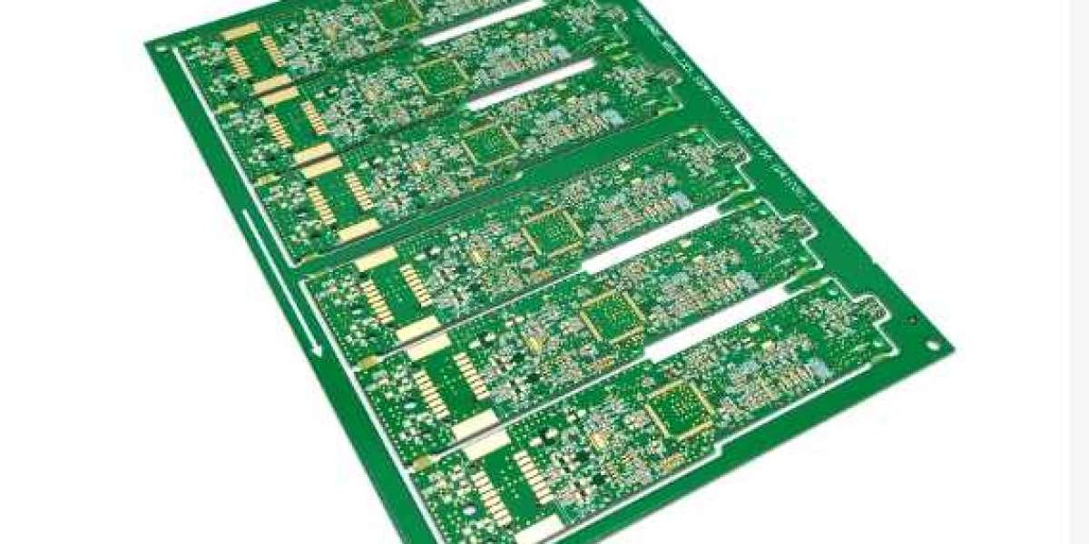
PCB silkscreen (also called printing) is the non-conductive ink layer printed on the top and bottom of a PCB board, to show text, symbols, and identifiers. It’s used to guide assembly and testing, improve traceability, and other informations such as safety, notice, reminder, etc.
On the PCB stack, silkscreen sits on top of the solder mask (not on copper). That position matters: it’s exposed to handling, cleaning, and reflow heat, so process control determines whether it stays crisp or turns into smudged, faded markings.
Silkscreen matters most when:
● Your PCB board is dense (fine pitch, many parts, tight clearances)
● Mass production (repeatability is everything)
● The product needs other works, service, maintenance later (field troubleshooting)
● You have compliance/safety labeling needs
What Is PCB Silkscreen Printing?
PCB silkscreen printing is the process of applying a durable ink pattern—text and graphics—onto the PCB surface after solder mask, using screen printing, photo-imaged legend, or digital printing.
Silkscreen vs Solder Mask
Solder mask is a protective insulation layer that controls where solder can wet; it’s a “process control” and protection layer.
Silkscreen is the information layer that sits above the mask; it’s for guidance, identification, and traceability.
Silkscreen vs Copper Markings
Copper markings are part of the conductive layer (pads/traces). Silkscreen is non-conductive and does not carry current. That’s why silkscreen can safely label near circuitry—but only if clearances are respected.
What Typically Goes on the Silkscreen Layer?
A good legend file usually includes:
Reference designators (R1, C12, U3)
Polarity and orientation marks (+/−, diode direction, pin-1 indicators)
Test point IDs (TP1, TP2) and net names (optional)
Safety warnings (high voltage, hot surface zones)
Logos, serial numbers, revision codes, date codes
QR codes or data matrix codes (common for tracking)
Why PCB Silkscreen Is Critical in Modern Electronics Manufacturing
Assembly Accuracy and Yield Improvement
Silkscreen is basically “visual DFM.” When pick-and-place, hand placement, or inspection teams can instantly confirm orientation and reference IDs, it could reduce:
rotated components
incorrect polarity placement
misloaded BOM positions
rework loops that damage pads and solder mask
Even a small error in placement can be a major yield across thousands of boards.
Testing, Debugging, and Maintenance Efficiency
Silkscreen speeds up debugging because it reduces the time which engineers spend between the board and schematic:
● quicker probe targeting (test points and component IDs)
● faster fault isolation
● easier ECO verification (rev marks and version cues)
For products with service life expectations, readable legends could help technicians avoid “guessing” and identifying the designators quickly, which prevents accidental damage and improve efficiency.
Safety, Compliance, and Risk Reduction
Silkscreen is often where you reminder what matters for safety:
● high-voltage boundaries
● safety icons, warnings
● lead-free labeling or process IDs
● compliance-required identifiers (varies by product/market)
A missing or incorrect warning label can create real liability risk, not just inconvenience.
Branding, Traceability, and Anti-Counterfeiting
Beyond a logo, silkscreen can support traceability systems:
● lot tracking (serials, date, codes)
● revision management (Rev A/B/C)
● location codes for process tracing
● IDs/serial number
When there is a defect, traceability is how you could identify root cause quickly.
PCB Silkscreen Materials: Ink Chemistry and Performance Requirements
Silkscreen inks must survive handling, solvents, and reflow temperatures while staying readable clearly.
Base Ink Technologies
● Epoxy-based inks: widely used, strong adhesion and durability, perfect for standard production.
● UV-curable acrylic inks: cure quickly, sharper edges, often favored for high-speed and digital-friendly workflows.
The “best” choice depends on your manufacturing process and downstream cleaning/reflow conditions.
Pigments and Optical Performance
White legends often use titanium dioxide (TiO₂) for opacity.
Black legends rely on carbon black or organic pigment blends.
Key requirements:
strong contrast against mask color
stable color after heat exposure
resistance to fading and staining
Functional Additives
Inks are engineered with:
flow control agents to prevent bleeding
thixotropic modifiers to hold shape
adhesion promoters for better bonding to mask
thermal stabilizers for reflow durability
Common Colors and Visibility Rules
White: most readable on green/black mask
Black: common on white mask
Yellow: used for special visibility cases, but must be controlled to avoid low contrast
Readability is not aesthetic—it’s operational. A “nice-looking” legend that becomes unreadable after reflow or even fades way, surely is not reliable.
PCB Silkscreen Printing Technologies
Manual Screen Printing
A mesh to transfers ink onto the PCB board surface.
● Pros: low setup complexity, cost-effective for simple boards
● Cons: limited resolution, alignment fluctuation, not ideal for very dense legends
● Best for: simple boards, prototypes, low-density layouts
Liquid Photo Imageable (LPI) Legend Printing
Uses a photo-imaging workflow (exposure + development) similar in spirit to solder mask imaging.
● Pros: better alignment and edge quality, suitable for mass production
● Cons: process steps are more involved than basic screen print
● Best for: consistent production with moderate-to-high density markings
Direct Legend Printing (DLP / Inkjet)
A digital CAD-to-board approach that prints ink directly.
● Pros: quick iteration, no screens, flexible for revisions
● Cons: equipment/ink compatibility limits, sometimes higher per-board cost at scale
● Best for: mixed builds, rapid changes, medium volumes
LDI for Legends
Laser Direct Imaging is mostly known for imaging steps, but the same mindset—accurate alignment—can be applied to legend workflows depending on the factory setup.
● Pros: alignment advantages on dense boards
● Best for: high-density PCBs where registration is tight
Comparison of PCB Silkscreen Printing Methods
Here's a practical "buyer's view" comparison.
Method | Minimum Text/Line | Alignment | Durability | Cost | Best Use |
Screen Printing | Moderate | Good (depends on setup) | Good | Low | Simple boards, stable layouts |
LPI Legend | Smaller text possible | Very good | Very good | Medium | Mass production, denser layouts |
DLP/Inkjet | Fine features possible | Excellent (digital) | Good–very good | Medium–high | Frequent revision, mixed builds |
LDI-assisted | Fine features | Excellent | Very good | Higher | High-density boards, strict registration |
Actual minimums depend on the manufacturer’s capability. The safe approach is always to confirm DFM limits before release.
PCB Silkscreen Printing Process: Step-by-Step Manufacturing Flow
This is the PCB silk screen printing process in practical terms, from data to inspection.
Silkscreen Artwork Design File Preparation
The legend layer is typically generated from CAD software like AltiumDesigner, KiCad, or Eagle.
Key preparation checks:
● clear, simple fonts
● avoid ultra-thin strokes
● ensure polarity and pin-1 marks are unambiguous
● place revision/serial fields logically (not under components)
PCB Surface Preparation
Even though silkscreen prints onto solder mask, surface prep still matters:
● remove dust and residues
● ensure surface is stable for adhesion
● confirm the board is dry and clean before printing
Ink Application Methods
Depending on the line:
● screen print transfers ink through a patterned mesh
● photo-imaging defines legend with exposure/development
● inkjet deposits directly from digital data
This is where the most common quality issues begin: too much ink, poor viscosity control, or marginal clearances.
Curing and Hardening
Legend durability depends on curing:
● Thermal cure: controlled temperature/time hardens the ink matrix
● UV cure: polymerization locks in the shape quickly
Under-cure causes smearing and poor adhesion; over-cure causes brittleness or poor bonding, depends on chemistry.
Inspection and Quality Verification
Typical inspections include:
visual legibility and completeness
AOI alignment and placement verification
verification of polarity and pin-1 marks
confirmation nothing intrudes into solderable pads or via openings
If the legend creates assembly risk, it’s not “cosmetic”—it’s a defect.
PCB Silkscreen Design Rules
Good DFM here prevents 80% of legend issues.
Minimum Font Size and Line Width
Design constraints should match printing method. If the PCB board is dense, keep text larger and prioritize what must be readable.
Practical rule: make reference designators readable at arm’s length under normal lighting. If you cannot read it clearly and have to read with a microscope, then that will slow down the manual works in future.
Guidelines of Placement and Clearance
● keep legend not on the pads and do not conflict with other areas, such as where a label will be attached
● avoid printing over via openings unless intentionally allowed
● leave space around fine-pitch footprints
● don't place critical marks where components will cover them
Single-Side vs Double-Side Silkscreen
● single-side printing is cheaper and usually enough for demands
● bottom legend is useful for boards assembled on both sides
● if your bottom side has dense components and have to be mounted by SMT, bottom legend must be prioritized carefully
Silkscreen Prioritization for Dense Boards
If you can’t fit everything, prioritize in this order:
● safety/compliance marks
● manufacturer ID + revision
● assembly reference and orientation
● test points (only the critical ones)
Common PCB Silkscreen Defects and How to Fix Them
● Smearing/bleeding: ink viscosity too low, surface not prepared, or under-cure
Fix: viscosity control, better preparation, correct cure profile
● Fading after reflow: ink chemistry not matched to reflow conditions, or weak cure
Fix: qualify ink system, validate post-reflow readability
● Misalignment: positioning drift, poor fiducial, or process variation
Fix: better alignment strategy, strict process controls, DFM clearances
● Poor adhesion/peeling: contamination, moisture, inadequate curing
Fix: improve cleaning/drying, refine cure window
● Illegible fine text: design too small or too close to features
Fix: increase font size, simplify content, prioritize critical marks
PCB Silkscreen Cost Breakdown and Optimization
Silkscreen is rarely a big item, but it can drive hidden cost through rework and scrap.
Cost drivers include:
● tooling/setup (for screens)
● print time and inspection load
● number of colors
● single vs double-side printing
● density and readability requirements (tight alignment adds process control)
Optimization strategies:
● Stick with one color unless there’s other reasons or considerations
● avoid printing non-essential text on dense boards
● standardize legend conventions across product families
● include clear revision/date/serial fields for traceability
DIY PCB Silkscreen vs Professional Manufacturing
DIY Silkscreen Printing
DIY can work for:
one-off prototypes
educational builds
simple designs with large markings
Limitations:
alignment stability
durability through reflow and cleaning
repeatability across batches
Professional PCB Silkscreen Services
Factory legend printing brings:
consistent alignment and curing
controlled materials
inspection standards that catch issues early
better readability for assembly lines
If your board is headed for production, professional legend control is usually cheaper than repeated rework.
How to Choose the Right PCB Manufacturer for Silkscreen Quality
When evaluating a supplier, ask:
● which legend methods they support (screen/LPI/inkjet)
● their minimum readable text and line width capability
● how they handle dense boards (DFM feedback, priority suggestions)
● what inspection is included (AOI vs visual)
● how quickly they communicate for legend conflicts (pads/vias/clearances)
A good manufacturer treats the legend layer as part of assembly yield—not just simple words.
PCB Silkscreen Industry Trends and Future Developments
Silkscreen used to be an “afterthought layer.” Today, it’s being pushed by the same forces reshaping the entire PCB manufacturing process: smaller hardware, faster production cycles, and higher traceability expectations.
● Miniaturization is squeezing the legend layer
As component pitch shrinks and boards get denser, there’s simply less space for readable text. Manufacturers are responding with finer printing capability, better registration control, and stricter DFM rules (larger fonts where possible, smarter prioritization, and cleaner keep-out zones around pads and vias).
● Automation + AI-driven inspection is becoming standard
More factories are using AOI to check legend alignment, missing marks, smearing, and encroachment on solderable areas. The trend is moving from “spot checks” to consistent, data-driven inspection—so legend defects are caught early and linked back to process parameters.
● UV-LED curing is replacing older curing approaches in many lines
UV-LED systems improve cure consistency, reduce heat load on the board surface, and support higher throughput. For silkscreen durability, stable curing is often the difference between crisp markings and legends that fade or scratch during handling.
● Environmental-friendly ink systems and cleaner processing are gaining attention
Environmental compliance is pushing ink and cleaning chemistry toward lower-VOC formulations, improved waste handling, and more efficient curing. The goal is less chemical load without sacrificing adhesion or readability after reflow.
● Global PCB demand is reshaping “legend requirements”
As production scales across consumer electronics, automotive, industrial, and medical applications, silkscreen is increasingly expected to support traceability (serials, QR/data matrix codes, revision control) and consistent labeling across multi-site manufacturing—especially for products that require field service and long lifecycle support.
PCB Silkscreen Printing FAQs
Is silkscreen mandatory?
Not mandatory, but strongly recommended for assembly efficiency, testing, and traceability.
Does silkscreen affect electrical performance?
Not electrically—if it stays off pads and critical areas. The risk is process/assembly interference, not conductivity.
Why does silkscreen fades after reflow?
Common causes include contamination, moisture, under-cure, or ink not matched to your reflow conditions.
Can silkscreen be corrected?
Minor touch-ups may be possible, but full corrections usually require process adjustment. For production, correction-by-rework is risky.
What is the minimum readable text?
Depends on printing method and inspection conditions. Always align legend process with your manufacturer’s capability and production constraints.
Conclusion: Best Practices for Reliable PCB Silkscreen Printing
PCB silkscreen isn’t decoration—it’s a functional layer that directly supports assembly accuracy, inspection efficiency, maintenance, and traceability. When it is treated seriously, it reduces rework, prevents placement mistakes, and makes field support faster, safer and efficient.
The most reliable results come from alignment across three areas:
● Design: clear, readable legend artwork with proper clearances and priorities for dense layouts.
● Material: inks matched to the solder mask, surface finish, and expected thermal/chemical exposure.
● Process: stable printing registration, correct curing, and inspection that catches defects before boards reach assembly.
Just as important is early collaboration between designers and manufacturers. A quick legend-focused DFM review can prevent common issues like text on pads, missing polarity marks, unreadable fonts, or silkscreen that degrades after reflow.
Applicable recommendations to lock in quality:
● Prioritize critical marks first: polarity, pin-1, reference designators, safety labels, and traceability codes.
● Follow method-based DFM rules for minimum font size, line width, and spacing—don’t simply rely on “what worked before.”
● Keep silkscreen away from solder areas, vias, and fine-pitch pads; add keep-outs reminder where needed.
● Specify legend requirements clearly in fabrication notes (color, side, durability needs, inspection expectations).
● Confirm curing and inspection controls with your manufacturer—consistent cure is key for adhesion and readability.
If you’re planning to manufacture PCB boards, Benlida Circuit can support both DFM feedback and production consistency as part of it’s PCB Fabrication Service — supporting your legend layer stay clear, from prototype to volume manufacturing.
Related PCB manufacturing processes
PCB Manufacturing Process Step-by-Step
PCB Inner Layer Imaging Etching Process
What is the PCB Lamination Process?
How do drilling (mechanical/laser) processes work in PCB manufacturing?
What is the plating process in PCB Manufacturing?
How is solder mask applied on PCB?
What is the surface finish process in PCB?
What are the most common methods of PCB testing?
About the auther:

Sonic Yang
As a major of Electronics and Mechanical Automation, Sonic has been engaged in PCB design, RD, manufacturing of eletronics for around 22 years, as engineering director and coordinates with supply chain(componentsCNC parts), providing professional supports and consults for global customers.